The micro-fabrication lab is a class 1000 clean room that mainly provides thin film processing machines to assist the research of optoelectronic components, quantum components, sensors and micro-fluidics.

感應式耦合電漿蝕刻系統
Oxford ICP-RIE
- Etched material:non metal
- Gas:O2, CHF3
- Etching pressure:1-10 mTorr
- Minimum deposition pressure:
200-2000mTorr - Plasma generation:
Upper Electrode 15V
Lower Electrode -15V - Sample Size:4" wafer
- Usage Fee:NT$ 1000/h

電子束蒸鍍系統
Ulvac E Beam Evaporator
(for
oxide)
- Material:Oxide
- Gas:O2
- Minimum vacuum:~10-7 torr
- Operating pressure:5×10⁻⁶ torr
- Maximum pressure:3×10⁻⁵ torr
- Heating temperature:150℃
- Rotation rate:15 rpm
- Sample size:4" wafer×3
(the wafer can be diced to a minimum
of 1×1 cm2) - Usage Fee:NT$ 800/h

電子束蒸鍍系統
FU-23 E Beam Evaporator
(for
metal)
- Material:Metal
(Au, Ag, Al, Ti, Cr, Ni) - Minimum vacuum:~10-7 torr
- Operating pressure:5×10⁻⁶ torr
- Maximum pressure:3×10⁻⁵ torr
- Heating temperature:150℃
- Rotation rate:0-25 rpm
- Sample size:4" wafer×3
(the wafer can be diced to a minimum
of 1×1 cm2) - Usage fee:NT$ 800/h

熱蒸鍍系統
Ulvac Thermal Evaporator
- Material:metal and non metal
- Base pressure:~10-4 Pa
- Operating pressure:4×10⁻⁴Pa
(3×10⁻⁶ torr) - Evaporation temperature:150℃
- Srate:none
- Sample size:4" wafer×1
(the wafer can be diced to a minimum
of 1×1 cm2) - Usage fee:NT$ 500/h

射頻/直流濺鍍系統
RF/DC Sputter
- Material:metal and non metal
- Source:2 DC-gun & 1 RF-gun
- Target Size:3 inch
- Gas:Ar, O2
- Base pressure:~10-6 torr
- Operating pressure:1-50 mTorr
- Spin Rate:15 rpm
- Sample size:4" wafer×1
(the wafer can be diced to a minimum
of 1×1 cm2) - Usage Fee:NT$ 500/h

直流濺鍍系統
TIRI DC Sputter
- Material:metal and non metal
- Source:1 DC-gun/ 2 DC-gun
- Target size:2/3 inch
- Gas:Ar
- Base pressure:~10-6 torr
- Operating pressure:1-50 mTorr
- Spin rate:10-90 rpm
- Sputtering temperature:non/700 ℃
- Sample size:4" wafer×1
5×5cm2 ×4
2.5×2.5cm2 ×6
(the wafer can be diced to a minimum
of 1×1 cm2) - Usage Fee:NT$ 500/h
Remarks
- Please bring your own materials. If you need to borrow materials held by our laboratory, a material fee will be charged: NT$ 10/nm.
- Available metal materials: Au, Ag, Al, Ti, Cr, Ni.
- Available oxide materials: Al2O3, SiO2, NiO.
- If the materials are not the above, please report to the manager first and make a note on the usage record.


The Advanced Fabrication Lab is a Class 1000 cleanroom located in room 4B19 of the IRBST. It primarily provides lithography equipment to support researchers within the center and the institute in the research and development of optoelectronic devices, quantum devices, sensors, and microchannels.
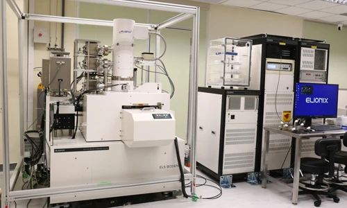
E-beam Lithography
ELS BODEN100
- Accelerating Voltage:100 kV
- Exposure Current:20 pA - 100 nA
- Scanning Speed:200 MHz
- Main Chamber Vacuum:≤ 4 × 10⁻⁴ Pa
- Electron Beam Diameter:φ 1.8 nm
- Minimum Line Width:6 nm
- Writing Field Size: 100 µm、250 µm、500 µm、1000 µm (at standard field)
- Scanning Resolution:Minimum resolution 0.2 nm
- Writing Area:X ≤ 210 mm,Y ≤ 210 mm
- Applicable Substrate Size:Wafer pieces to 8-inch wafers
- Usage Fee:NT$ 1500/h

FIB/SEM dual beam system
Helios 660
- SEM:G4column
- Resolution:Sub-nanometer from 1 kV to 30 kV
- Features:High-resolution triple in-lens electron detectors, including a Through Lens Detector (TLD, secondary and backscatter mode), an In-Column Detector (ICD, low-loss backscatter), a Mirror Detector (MD, no-loss backscatter), and a CBS (circular back scattering) detector.
- Ion Beam:Gallium (Ga) ion source
- Operating Voltage:5 - 30 kV
- Current Range:1.1 pA to ~nA level
- Features:Gas Injection System (GIS) available for Platinum (Pt) metal deposition
- Usage Fee:NT$ 3000/h
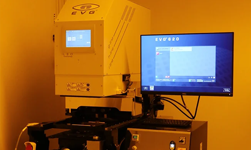
Mask Aligner EVG620 NT
- Light Source Power:UV LED (1000W)
- Light Source Wavelength:I-line 365nm / H-line 405nm / G-line 436nm
- Substrate Sizes:Wafer pieces, 2" - 6" wafers
- Usage Fee:NT$ 1000/h
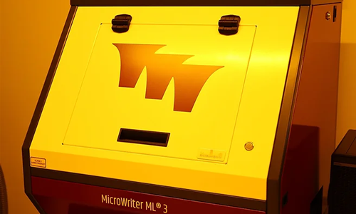
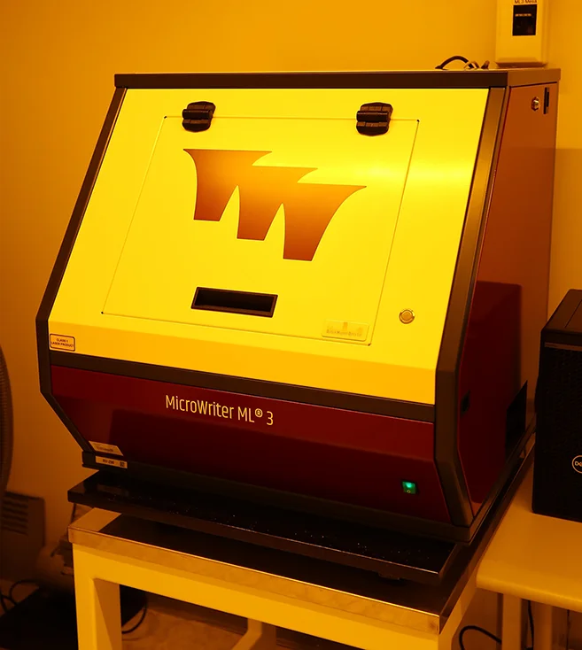
ML3 Mesa direct writer
- Light source:UV LED
- NUV:365nm / 405nm
- Substrate Sizes:2" - 6" wafers, 155mm x 155mm
- Resolution:0.6μm / 1μm / 5μm
- Writing speed:
17mm2/min (0.6μm resolution)
50mm2/min (1μm resolution)
180mm2/min (5μm resolution) - Usage Fee:NT$ 800/h
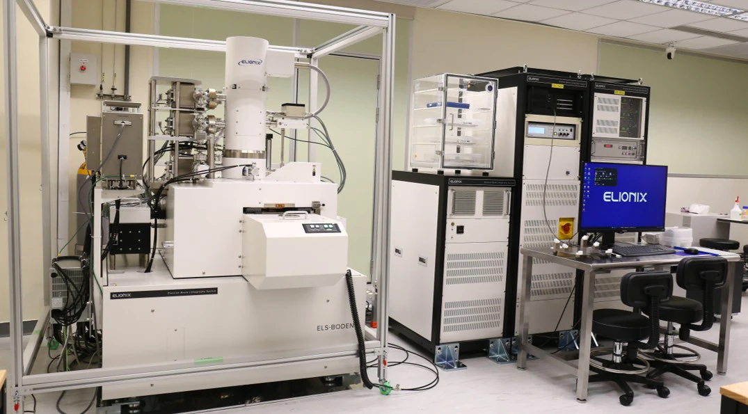


- Interdisciplinary Research Building of Science and Technology B2C03
(Micro Fabrication Lab) - Interdisciplinary Research Building of Science and Technology 4B19
(Advanced Fabrication Lab )
- Passed the laboratory safety and health training course of Academia Sinica.
- Download and read the lab introduction and how to use it yourself.
- After submitting the application form, the administrator will conduct on-site safety training.
- Assessment will be based on the lab introduction content, usage regulations and on-site safety training content.
- Access control permission will be issued after passing the assessment; those who fail will have to apply for another assessment one month later.
- After obtaining the access control, you can apply for machine training, and then take the exam to obtain the machine use permission.
Laboratory Manager: Ms. Chia-Chu Kuo
EBL/FIB Instrument Manager: Ms. Jia-Wern Chen
Mask Aligner/Direct Writer Instrument Manager: Mr. Wei-Hao Liao
Laboratory Principal Investigator: Dr. Shu-Yi Hsieh
Please feel free to add comments to the paper if you have any research results produced by using the
core facilities of RCAS:
Technical support was provided by Core Facilities of Research Center for Applied Sciences (RCAS), Academia Sinica (Project No. AS-CFI-113-A10).
(If any related research results are published, please kindly provide the publication
information to the facility manager. Thank you.)
- Research Center for Applied Sciences Yi-Chung Tung, Research Fellow
- Research Center for Applied Sciences Shih-Yen Lin, Research Fellow
- Institute of Chemistry Hsiung-Lin Tu, Associate Research Fellow
- Institute of Physics Chung-Ting Ke, Assistant Research Fellow
- Research Center for Critical Issues Yen-Chun Chen, Assistant Research Specialist