Redesigning Two-Dimensional Semiconductor Interfaces at the Atomic Scale through Epitaxial Interface Engineering
Summary of Achievement
Two-dimensional (2D) semiconductors are promising candidates for next-generation electronics because their atomically thin structure enables continued device scaling beyond the limits of conventional silicon technology. However, their electronic performance is highly sensitive to the quality of the interface with surrounding dielectric materials, making interface engineering a key challenge for practical applications.
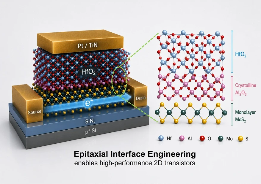
Led by Distinguished Research Fellow Wen-Hao Chang at the Research Center for Applied Sciences, Academia Sinica, the research team developed a new epitaxial interface engineering strategy to precisely tailor the atomic-scale interface between monolayer MoS₂ and the gate dielectric. The resulting top-gate transistors demonstrated outstanding transconductance, low leakage current, and excellent device uniformity at a channel length of approximately 100 nm. This work establishes a new approach for advancing 2D semiconductor devices and future post-silicon electronics, and was published in Nature Electronics.