Multiscale Molecular Simulation and Machine Learning Join Forces to Enable the Wafer-scale Epitaxial Growth of High-mobility p-type Boron Carbon Nitride (BCN) 2D Semiconductors
Summary of Achievement
Two-dimensional (2D) semiconductors, owing to their atomic-scale thickness, are regarded as a key material to overcome the scaling limits of conventional silicon electronics and to realize next-generation devices. Yet high-performance p-type 2D materials have long remained elusive, mainly because such materials generally exhibit strong electron-doping tendencies, orbital localization and pronounced hole scattering, which prevent the realization of stable and efficient p-type 2D semiconductors and, in turn, hinder the development of three-dimensional complementary field-effect transistors (CFETs). Growing high-quality, stably p-type 2D semiconductors at the wafer scale has therefore been a central challenge in the field.
A cross-disciplinary team led by Dr. Chun-Wei Pao at the Research Center for Applied Sciences, Academia Sinica, together with National Taiwan University and the University of Tokyo, proposed a chemical vapour deposition (CVD) strategy centred on precursor engineering, and successfully grew wafer-scale, monolayer boron carbon nitride (BCN) epitaxial films on single-crystal Cu(111). Using monomethyl ammonia borane (MMAB) and ammonia borane (AB) as dual precursors, the team tuned their dehydrogenation and surface-reaction pathways to overcome the spatial and temporal mismatch in the delivery of boron, carbon and nitrogen atoms, so that carbon atoms are incorporated primarily by substituting nitrogen sites (C_N) within a continuously crystallized boron nitride lattice. The resulting monolayer BCN has a bandgap of about 1.90 eV, and the wafer-scale arrays of p-type BCN field-effect transistors exhibit a hole mobility of 100 cm2 V-1 s-1, an on-current above 0.9 mA/um and an on-off ratio of 10^8, surpassing the current state of the art among p-type 2D semiconductors.
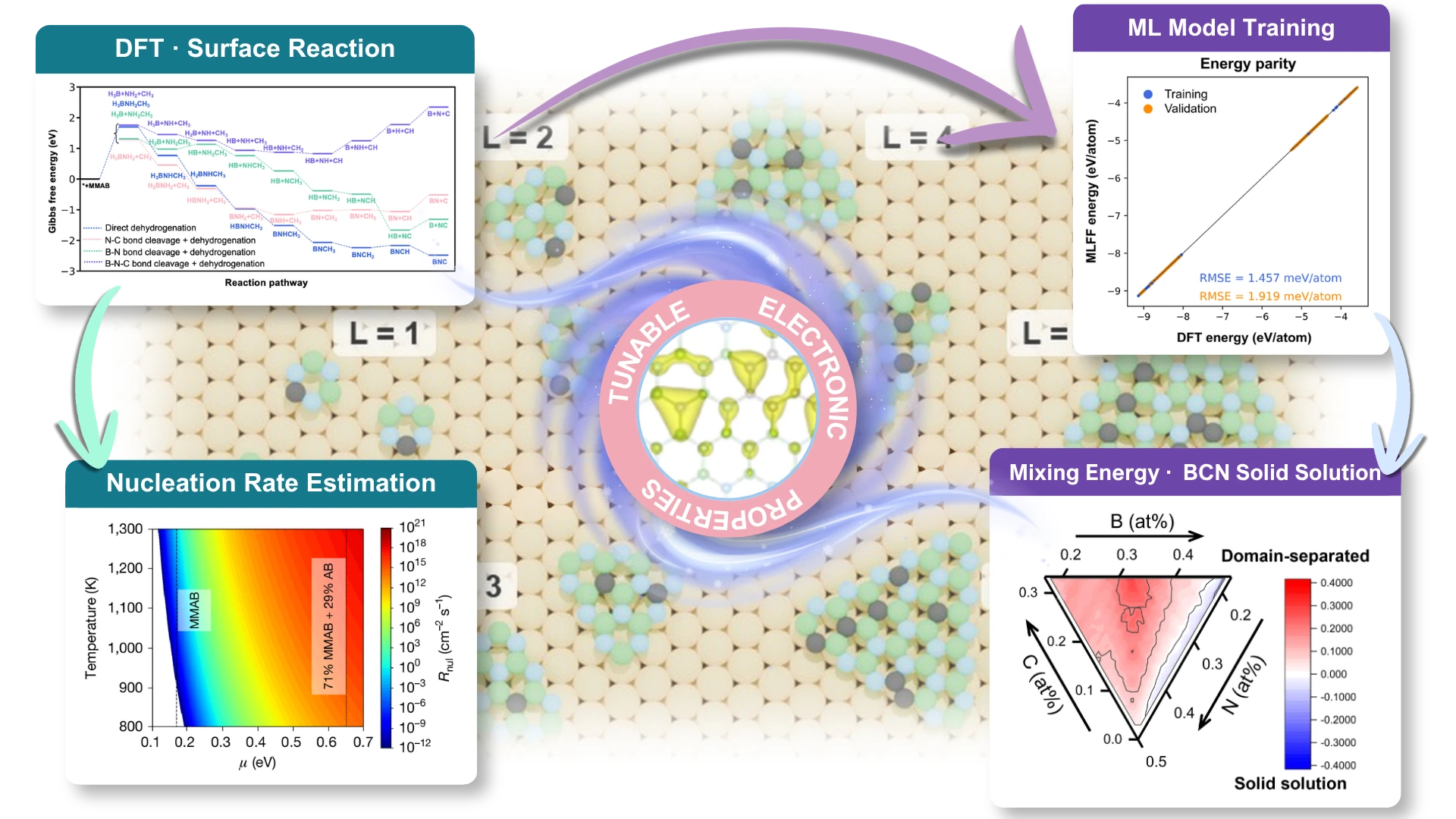
In this work, Dr. Pao's team was responsible for the multiscale molecular simulation and machine learning, playing a pivotal role from microscopic mechanisms to help process design. First, they used first-principles density functional theory (DFT) to calculate the decomposition and surface-reaction pathways of MMAB and AB on Cu(111), clarifying the competition between dehydrogenation and N-C/B-N bond cleavage and confirming that the "dual-precursor slow-release" strategy effectively resolves the spatial and temporal mismatch in B, C and N delivery. Combined with classical 2D nucleation theory, they further constructed a nucleation-rate map versus temperature and chemical potential to guide the optimal growth window. To overcome the cost and length-scale limits of DFT, the team trained a machine-learning force field (MLFF) based on the DeePMD-kit framework, using more than 8,000 DFT structures to obtain a deep-potential model whose prediction errors for energy and atomic forces are below 1.919 meV/atom and 0.111 eV/Angstrom, respectively. Leveraging this efficient MLFF, they generated more than 12,000 BCN configurations - each containing 2,592 atoms on a 36x36 Cu(111) surface - computed mixing-energy (Emix) ternary diagrams, and performed Monte Carlo sampling, establishing that there exists stable quasi-random solid solution BCN phase composed of isolated carbon atoms and graphene-like nanodomains, rather than global phase separation - a key structural insight that explains the material's electronic properties. Finally, using the HSE06 functional they obtained a theoretical bandgap of 1.92 eV, in agreement with the 1.90 eV measured by scanning tunnelling spectroscopy, and showed that the p-type behaviour and narrow bandgap originate from carbon substitution at isolated nitrogen sites and the graphene-like nanodomains.
Collectively, this work establishes a simulation-synthesis-device loop in which multiscale molecular simulation and machine learning provide complete theoretical support from atomistic reaction mechanisms to large-scale solid-solution phase stability, enabling the realization of wafer-scale, high-mobility p-type BCN 2D semiconductors and offering a key materials platform for three-dimensional complementary electronics in the post-silicon era. The results were published in Nature on 30 September 2026.